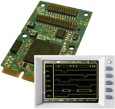
PCIE FPGA bridge
PCIe to simple IOBUS for Cyclone IV and Mini Pcie Fpga
PCIE to IOBUS SDK
PCIe to General Pourpuse I/O Bus Bridge (PCIe target), Drivers, QSYS and Demo Sources
The GPIO-BUS interface provides a parallel bus with 32 bits data lines, 8 bit address bus lines, controls (RD#, WR#, CS0# , CS1#), auxiliary signals (WAIT#, INT#).
The bus cycle timing can be defined by a control register, setup, hold and pulse width can be changed by user allowing bus cycle time from 48ns to 768ns with 16ns steps. Additional delay can be added by WAIT# signal.
The system includes VHDL source, QSYS design, command line demo source and executable, fpga loadable files (both EP4CGX15BF14C7N and EP4CGX30BF14C6N fpga).
The loading of system on the FPGA needs an USB blaster, some PCIE board (mini PCIE and PCIE on cables) require also a MBBA adapter.
- Click here to open data sheet
- Click here to view all documents list
Buy Online
- 141030-01A1 MS-Windows 32bits, XP and Seven version
- 141030-01A3 MS-Windows 64bits, Seven version
- 141030-01A4 Linux64 version


