PCIe FPGA Systems
Ready to start basic system with DMA and Drivers
Brief about PCIE to IOBUS SDK
PCIE Bridge to a simple parallel bus
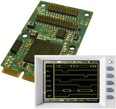
The GPIO-BUS PCIe bridge provides a parallel bus with 32 bits data lines, 8 bit address bus lines, controls (RD#, WR#, CS0# , CS1#), auxiliary signals (WAIT#, INT#). The bus cycle timing can be defined by a control register, setup, hold and pulse width can be changed by user allowing bus cycle time in range 48-768ns with 16ns steps. Additional delay can be added by WAIT# signal. The system includes VHDL source, QSYS design, demo source and executable, fpga loadable files, linux or windows drivers.
PCIe I/O registers SDK
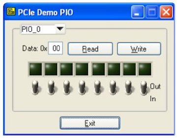
The PCIE register system SDK is targeted for help the designers in the starting phase of projects that requires controll PCIe mapped registers used both to control I/O pins or internal logic. The SDK includes the drivers and some demo and examples, avoiding a lot of startup issues.
PCIe Dma System SDK
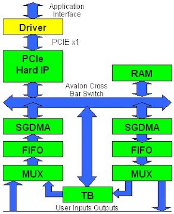
The present basic system is targeted for help the designers in the starting phase of projects that requires fast DMA straight way in PC virtual memory. It includes a QSYS system with 2 SGDMA configured one in input and one in output that can be wired to your application hardware, a TB Pheripheral can be used to test the system and measure the performances, drivers, and demo program.


