Creating PCI Express on FPGA
How you can design and simulate a PCIe on a FPGA. (Corso su come implementare il PCIe su FPGA)
VEC222E: Intel Fpga PCIe IP uses
Fpga programming courses series
Do you want to expand your embedded PC by adding input and output ports on PCIe®? Are you beginning or working on a design that uses one or more PCI Express®; interfaces? Do you have questions regarding bringing up your FPGA’s PCIe link?
Then this course should be of interest to you!
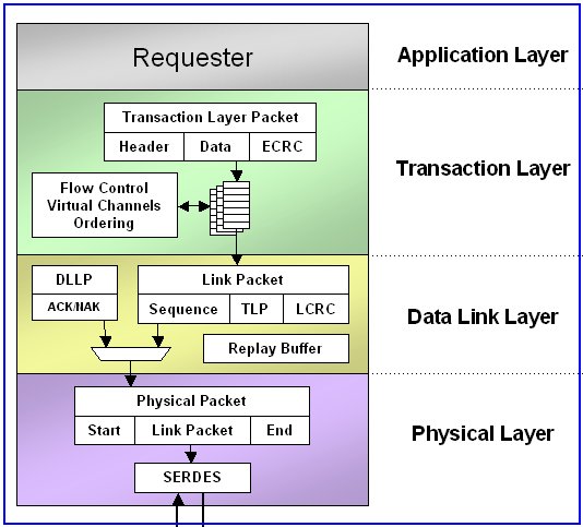
We’ll start with a high-level overview of the PCI Express protocol and from there you’ll learn the design flow to target the Hard IP for PCI Express blocks found in Cyclone® V, Arria® V and Stratix® V devices, particularly when using the Qsys system design tool.
You’ll see how to debug and test your PCIe links, both through simulation and in-system. You’ll discover advanced device features to add more flexibility and capability to your PCI Express-based design.
By the end of the training, you’ll feel comfortable getting your own device’s PCIe link up and running.
Course duration: 2 days
At Course Completion you will be able to:
- Describe the features and functionality of the Hard IP for PCI Express.
- Build a PCI Express solution targeting an FPGA using the Qsys system development tool
- Generate a testbench to simulate the Hard IP for PCI Express and modify the testbench to perform custom tests
- Debug a PCIe link using Intel® debugging tools and transceiver features
Prerequisites:
- We recommend completing the following courses:
- VEC102, The Quartus Prime Software Design Series: Foundation
- Transceiver Basics
Skills Required:
- Some understanding of the PCI Express Protocol specification is helpful, but not required
- Familiarity with common high-speed transceiver architecture.
- Familiarity with FPGA/CPLD design flow
- Familiarity with the Quartus Prime design software
- Some familiarity with the Qsys design tool is helpful, but not required


